


Hokkaido University (President: Toyoharu NAWA), Sungkyunkwan University (President: Chung Kyu SANG), and The National Institute of Advanced Industrial Science and Technology (Chief Director: Ryoji CHUBACHI) found that the two-dimensional electron gas confined in GaN, which is blue LED material showing high electron mobility, exhibits high thermoelectric power factor, 3−4 times greater than that of practical thermoelectric materials. Two-dimensional electron gas is an extremely thin (a few nanometers) electron accumulated layer. Recently, high performance thermoelectric materials have been reported from USA and China. However, there is no practical thermoelectric device using those thermoelectric materials. We expect that the present finding may be useful to improve thermoelectric performance of those materials. This result has been published in the following paper (open access journal). Hiromichi Ohta*, Sung Wng Kim, Shota Kaneki, Atsushi Yamamoto, and Tamotsu Hashizume*, “High thermoelectric power factor of high-mobility two-dimensional electron gas”, Advanced Science 4, 1700696 (2017). [DOI: 10.1002/advs.201700696]
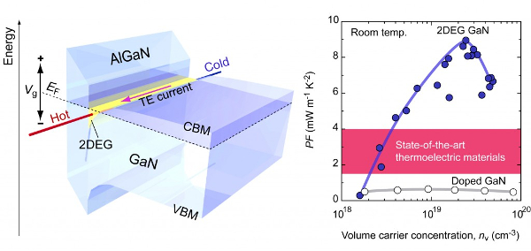
Thermoelectric conversion is an energy harvesting technology that directly converts waste heat from various sources into electricity by the Seebeck effect of thermoelectric materials with a large thermopower (S), high electrical conductivity (σ), and low thermal conductivity (κ). State-of-the-art nanostructuring techniques that significantly reduce κ have realized high performance thermoelectric materials with a figure of merit (ZT= S2∙σ∙T∙κ−1) between 1.5−2. Although the power factor (PF=S2∙σ) must also be enhanced to further improve ZT, the maximum PF remains near 1.5−4 mW m−1 K−2 due to the well-known trade-off relationship between S and σ. At a maximized PF, σ is much lower than the ideal value since impurity doping suppresses the carrier mobility. We prepared a metal-oxide-semiconductor high electron mobility transistor (MOS-HEMT) structure on an AlGaN/GaN heterostructure (Fig. left). Applying a gate electric field to the MOS-HEMT simultaneously modulates S and σ of the high-mobility electron gas from −490 μV K−1 and ~10−1 S cm−1 to −90 μV K−1 and ~104 S cm−1, while maintaining a high carrier mobility (~1500 cm2 V−1 s−1). The maximized PF of the high-mobility electron gas is ~9 mW m−1 K−2 (Fig. right), which is a two- to six-fold increase compared to state-of-the-art practical thermoelectric materials.
Original article
Contacts
Research Institute for Electronic Science
Hokkaido University
Email: hiromichi.ohta[at]es.hokudai.ac.jp
http://functfilm.es.hokudai.ac.jp/english/
Professor Tamotsu Hashizume
Research Center for Integrated Quantum Electronics
Hokkaido University
Email: hashi[at]rciqe.hokudai.ac.jp
http://www.rciqe.hokudai.ac.jp/en/